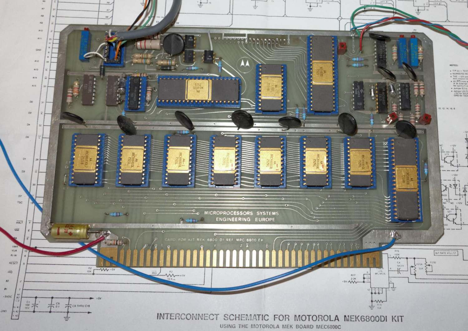
Luckily, the schematic diagram was still included in the documents : while its quality is not outstanding, it was a great help during the restoration process.Â
The M6800 family chips used in the board are presented below :
- 1 x CPU XC6800B 8-bit microprocessor. In the early days, Motorola used the prefix XC, instead of MC, for engineering prototypes. This chip has a 1 MHz max clock frequency and- as the others in this board- is housed in a ceramic DIP, with a gold top and gold pins.
- 7 x MCM6810L 128-byte static RAM. The first six RAM, addresses from 0 to 027F hex, are the RAM program memories. The user has the huge amount of 640 bytes for storing his program code. Yes, I'm talking about 640 bytes, not Gbytes, not Mbytes and not even kbytes ! Don't forget, we were in 1975.
The 7th MCM6810L (address at A000 hex) is used by the MIKBUG control program as a temporary storage and stack area.
-Â 1 x MCM6830L7. This is a 1024x8 mask-programed ROM, located at E000 hex. Two resident control programs, MIKBUG and MINIBUG are firmwares allowing the loading, debugging, and controlling of the user programs.
- 2 x XC6820 Peripheral Interface Adapters (PIA). XC prefix for engineering prototypes. This device is capable of interfacing the MPU to peripherals through two 8-bit bidirectional parallel ports and four control lines.
- 1 x MC6850L Asynchronous Communication Interface Adapter (ACIA). Used to interface the MC6800 to asynchronous serial devices.
Additional components are used for interfacing and/or controlling these chips : CPU and UART clock generation, connection to the external world, etc.
The board needs 3 power supplies : +5 V (1 A) for the M6800 chips and the logic glue, +12 and -12 V (# 100 mA) for the RS232 interface. RS232 rates are 110 or 300 Bauds but only 110 Bauds is available on this module. In 1975, the 110 Bds ASR33 Teletype®, with automatic reader and punch options, was the most frequently used terminal (20 mA loop current or RS232 V24).
Â
2. The first tests
After a thorough visual inspection and an ohmmeter check of the power supplies lines to detect any short-circuit, I connect the RS232 connector to my PC. I then run the Hyperterminal software (110 Bds, 8 bits, 1 Stop bit, No Parity, No Flux Control, VT100 emulation) and switch on the power supplies. After pushing the Board Reset switch, I can see a lot of weird characters on my PC screen : it seems that the RS232 bit rate is not correct.
The schematic shows that this speed is defined by a RC network connected to a MC14536 chip used as a timer : I try to adjust R (a 47kOhms potentiometer) to get a 9 ms half-period on TP4, as explained in the manual. No success !
I then suspect that C is the culprit : its value, according to my schematic, is 680 pF but the one on the board is a 1000 pF. A check with my capacitor meter says "300 pF""! I replace it with a new one, reconnect the board and push the Reset switch. I can now adjust R to read 9 ms on my scope. A "*" character is displayed on my PC screen showing that MIKBUG welcomes me and is ready to accept commands!
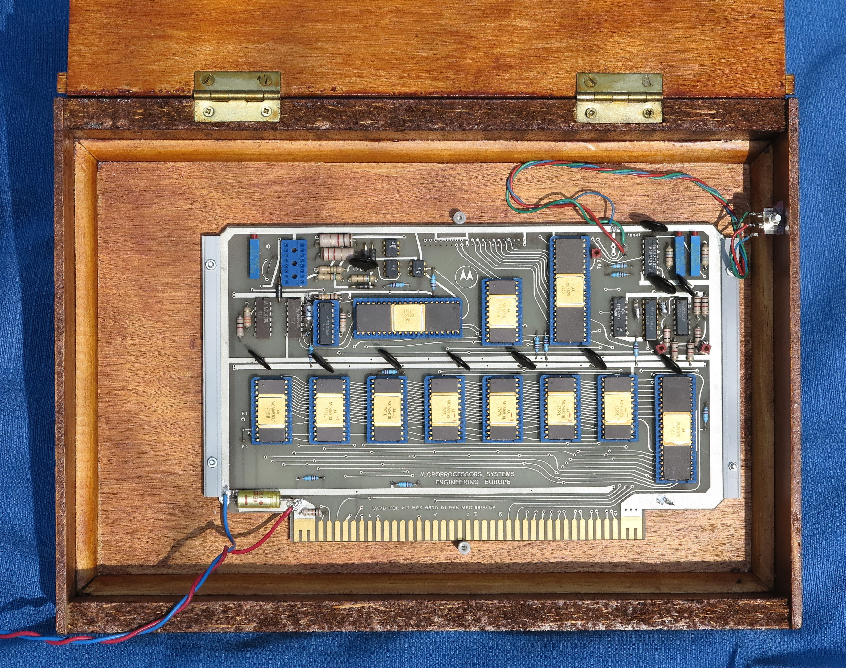
Before conducting more experiments, I put the evaluation module in a box to protect it against dust and shocks.
3. The first program
I'm now ready to write a short program and run it. In 1975, you had 3 ways to develop a program for this board :
- Use the Motorola Assembler on a GE Timeshared Service System or equivalent.
- Purchase an EXORCISER Motorola Development Tool.
- The simplest and cheapest way was to write M6800 assembly instructions on a sheet of paper, translate them into machine language hexadecimal bytes and then write these bytes into the RAM! There was not an assembler in the MIKBUG ROM, only RAM read and write commands and load, print and debug commands.
Nowadays, one can find several free assemblers accepting M6800 instructions and generating machine code in Motorola format, for instance :
http://sourceforge.net/projects/asm68c/http://www.hvrsoftware.com/6800emu.htm
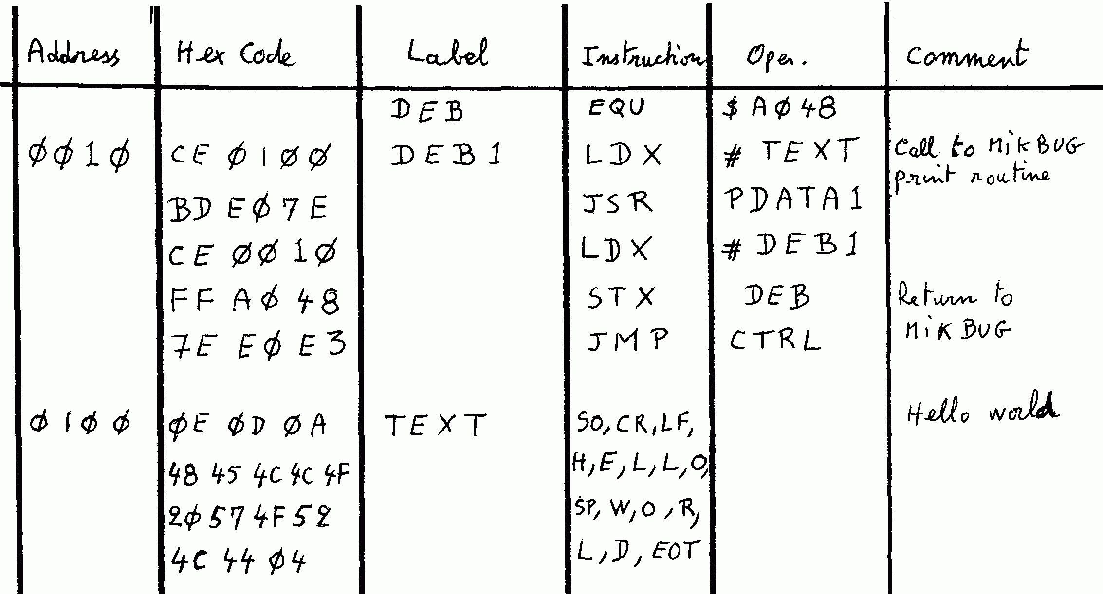
However, I choose to play the game as I did 40 years ago and to write machine code the old way. Here is a copy of the paper sheet of one of my recently hand-assembled small program displaying "HELLO WORLD" :
Â
This program makes use of the PDATA1 MIKBUG routine to display the ASCII string and of the CTRL routine to give control back to MIKBUG at the end.
The MIKBUG firmware enables the user to perform the following functions :
-Â
M : Memory examine and change.
-
R : Display contents of MPU Registers
-Â
P : Print/Punch memory
-Â
L : Memory Loader
-Â
G : Go to User's Program
We use theÂ
M command to write the machine Hex code bytes into the memory, beginning at address 0010 hex and ending at 001E hex. The ASCII string is written in the same way (
Mcommand) from address 0100 hex to 010E hex.
Then we write the beginning address of our program (0010 hex) into the Stack addresses A048 hex and A049 hex and typeÂ
G to run the program.
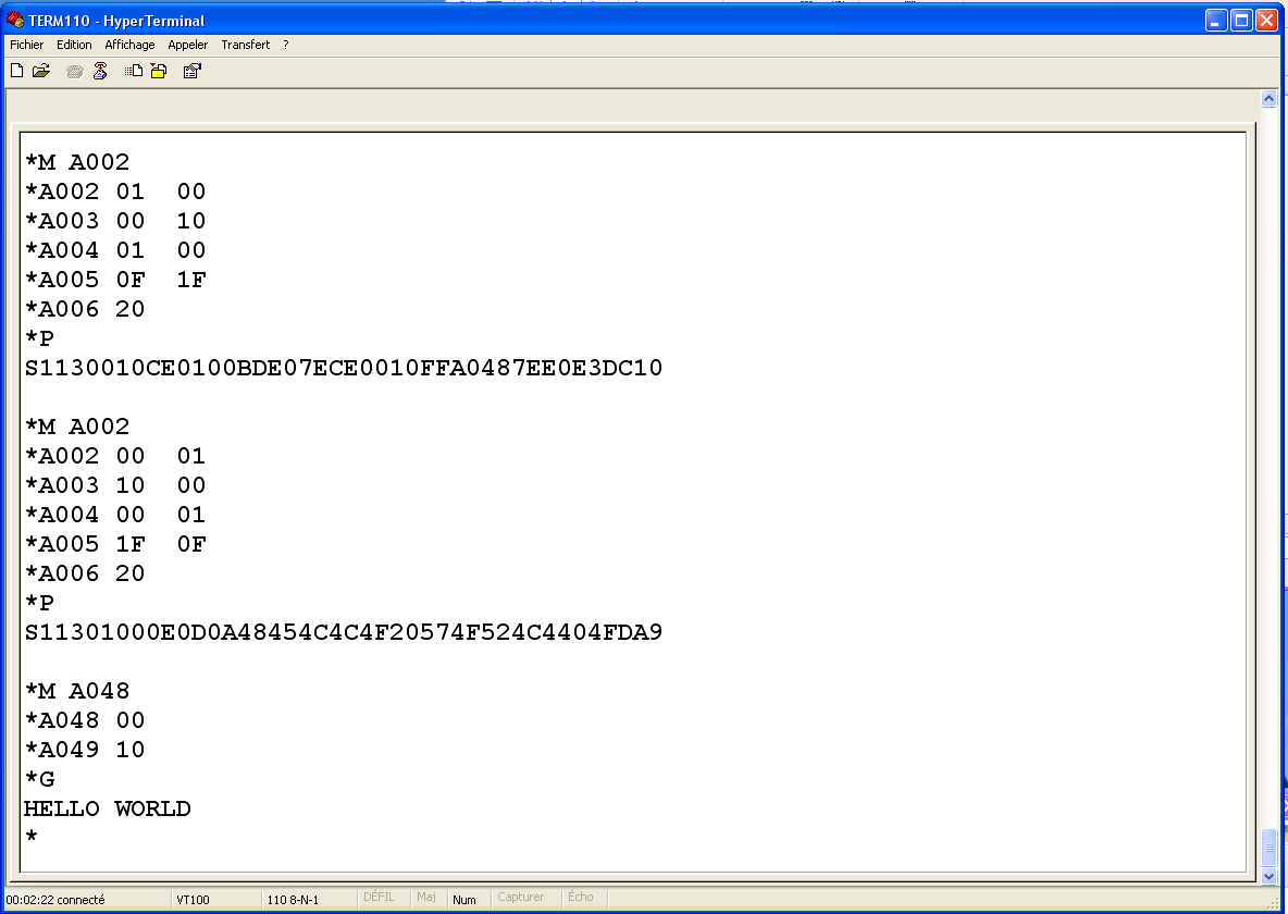
The picture below is a copy of the PC screen :
The first 17 lines show the contents of the RAM obtained with the
P command : from 0010 hex to 001E hex for the program and from 0100 hex to 010E for the text.
Then you see the Stack A048, A049 hex where I write the beginning address of my program.
TheÂ
G command runs the program which prints "HELLO WORLD" then gives control back to MIKBUG.
Conclusion
I'm very happy to bring the MEK6800D1 back to life after such a long sleep. A future work will be to fix the old ASR33 Teletype® terminal still in my garage, but this is a very different job, mainly mechanical because of rusted parts and dried grease and oil!



Afegeix-hi un comentari: