 Processor in Flip-Chip Pin Grid Array Package
Flip-chip assembly, also known as controlled collapse chip connection (C4), is a method of packaging and connection technology (AVT) for contacting unsealed semiconductor chips (bare die) by means of contacting mounds – so-called "bumps".
In flip-chip assembly, the chip is mounted directly, without additional lead wires, with the active contacting side facing downwards – towards the substrate/circuit carrier. Hence the name flip-chip. This results in particularly small dimensions of the housing and short conductor lengths. In the case of very complex circuits, this technology often offers the only sensible connection option, because in some cases several thousand contacts have to be realized. In this way, the entire surface of the die can be used for contacting, in contrast to wire bonding, where this is not possible or only possible to a very limited extent because the wires would cross each other and would very likely come into contact with each other. Furthermore, in wire bonding, the connections are made one after the other. With the flip-chip bonding technique, all contacts are connected at the same time. This saves time.
In addition to soldering and conductive bonding (see ICA and ACA), press welding (thermode bonding) is also used as a joining process to bond the chips.
Other package designs are listed under Chip Packages.
C4 Technology
C4 stands for the summary of the first letters of the terms "controlled collapsed chip connection" (= CCCC = C4).
C4 flip chip technology was introduced by IBM in 1964 and has undergone several modifications since then. This technique is used, for example, in the production of complex microprocessors. You can imagine the production as follows: The entire surface of the wafer is coated with a metal, e.g. by sputtering. Now a paint mask with defined openings is applied. Subsequently, the solder is deposited galvanically. The varnish mask is removed. This creates cylindrical solder bodies, as specified by the paint mask. These solder cylinders form the contact points that establish the connection to the circuit structures in the deeper layers of the wafer or each die. A selective etching process is used to remove the remaining metal layer that is not covered by the deposited solder. The solder cylinders are then melted into small balls (bumps) (reflow). The wafers are then separated into silicon chips. The chips are wetted with a flux and the structure is heated so that the solder melts and creates an electrical connection between the contact surfaces of the chip and the contacts of the substrate (package) (reflow soldering).
Another method of putting the bumps on a wafer is stencil printing. After the wafer has been electroplated to obtain a solderable surface on the pads, it is printed with solder paste in a stencil printer. The wafer is then subjected to a reflow process, the solder paste melts over and bumps are formed. The wafer can then be cleaned to remove flux residues. This is followed by the separation of the chips and the processing after wetting with flux in the SMD manufacturing process.
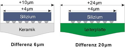
After soldering to the substrate (package) or the printed circuit board, the assembly requires a so-called underfill (an elastic, temperature-resistant plastic) so that the different coefficients of thermal expansion of the chip and substrate do not destroy the structure.
 Flip-chip assembly of a chip on different substrates (scheme)
After the underfill process, the flip chip looks like this:
 Flip-chip assembly with "underfill"
Bonding with non-conductive adhesive (NCA)
 NCA Technology
The technology is often referred to as the NCA (non-conductive adhesive) process . Here, the contacts of the chip are usually provided with so-called stud bumps, which are made of gold wire. The stud bumps are applied using the wire bonding process (ball-wedge method) and then torn off directly over the ball. In some cases, the bumps are then flattened using a special tool and brought to an even height (coining).
A non-conductive adhesive (usually epoxy-based) is applied to the substrate and the chip is pressed into it (bonded). The pressure during assembly must be sufficiently high for the stud bumps to penetrate the adhesive layer securely in order to be able to establish an electrical connection. The glue is then cured at an elevated temperature, with the tool with the chip under constant pressure. It is important for a secure bond that the adhesive shrinks as it dries, so that the bumps are drawn to the contact surfaces of the substrate and an electrical contact is formed.
Of all flip-chip assembly methods, NCA technology is the most suitable for small batches, as the bumping of the semiconductor chips is still possible even after the wafer has been separated. The assembly process is also well suited for low volumes. The achievable contact distances are quite small, which means that a high level of integration is possible. Due to the extensive course of the adhesive under the chip, there is no need for a separate underfill process.
Chip bonding under pressure results in a relatively high cycle time, as the placement tool requires a certain cooling time in order not to initiate the hardening process too early on the next part. Stud bumping is also not an ideal bumping process for large series, as serial ball bonding takes much more time than flat application processes such as screen printing or sputtering.
Bonding with isotropic conductive adhesive (ICA)
 Principle of ICA technology
This process is referred to as ICA (isotropic-conductive adhesive). An isotropically conductive adhesive is applied to the contacts of the substrate. Then the chip with its contacts (with bumps) is placed on the adhesive dots. The adhesive is cured thermally or by means of UV radiation to create a mechanical and electrical bond. Since the adhesive is not applied over the entire surface, an underfill is usually necessary after curing. In this process, the bumps are usually applied at the wafer level, e.g. by sputtering or vapor deposition of nickel. Stud bumps are possible, but rarely used.
Unlike the NCA or ACA process, the process does not have to be serial, which means that many chips can be cured in one pass. This leads to a reduced cycle time. The temperatures required for curing are usually lower than for soldering, so the thermal load on the component is lower.
This type of contacting is limited to a few and relatively large contacts, as the adhesive cannot be applied arbitrarily finely and also runs when the chip is placed. The process offers hardly any advantages over the soldering of flip chips, but requires an additional process, while soldering is integrated as a standard process in packaging and connection technology (AVT). For these reasons, this procedure is rarely used.
Bonding with anisotropic conductive adhesive (ACA)
 Principle of ACA technology
The process is called ACA (anisotropic-conductive adhesive). Anisotropic conductive adhesive consists of an adhesive that is weakly filled with small conductive particles of the same size, such as polymer balls coated with gold. The adhesive is applied over the entire surface of the contacts of the substrate. Due to the low fill factor of the conductive particles, they are not connected after application, so that there is no conductive layer that would short-circuit the contacts. When the chip is placed, the adhesive is displaced by the mechanical pressure and the conductive particles are compacted until they are sandwiched between bumps and substrate pads, creating a conductive bond. To ensure a secure connection, the pressure is maintained during the curing process. As with the ICA process, the bumps are usually created directly on the wafer.
One advantage is that the chip is bonded over a large area, so that an additional underfill process is no longer necessary. Furthermore, the achievable contact distances (pitch) are very small, significantly lower than with the ICA method. The pressure required during assembly is significantly lower than with the NCA process, which results in less mechanical stress.
One disadvantage, as with the NCA process, is that the chip has to be pressed against the substrate during the curing of the adhesive (thermocompression) so that the electrical contact is maintained, which has a negative effect on throughput. Also, ACA glue is relatively expensive due to its complex structure and small number of manufacturers.
Links


Comentaris publicats
Afegeix-hi un comentari: